Improved Ammeter Design Project Page
Description
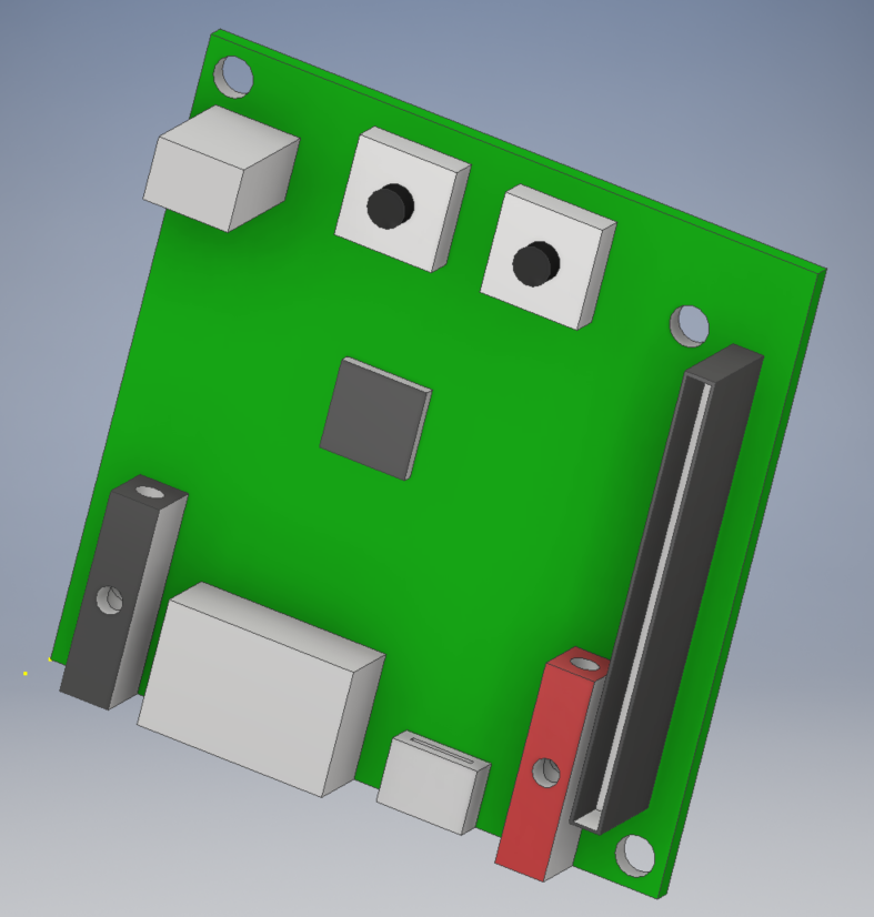
Project developed in Modern Circuit Board Design and Prototyping class taught by Prof Westerfeld. During this class, we designed circuits using eagle cad software and also designed and built 3d models using Autocad. An Improved current meter was designed and built for the final project. This current meter design is intended to minimize the effects of burden voltage that is present in the multimeters used in the lab and other facilites.
design and spec
Design drawing(initial version)
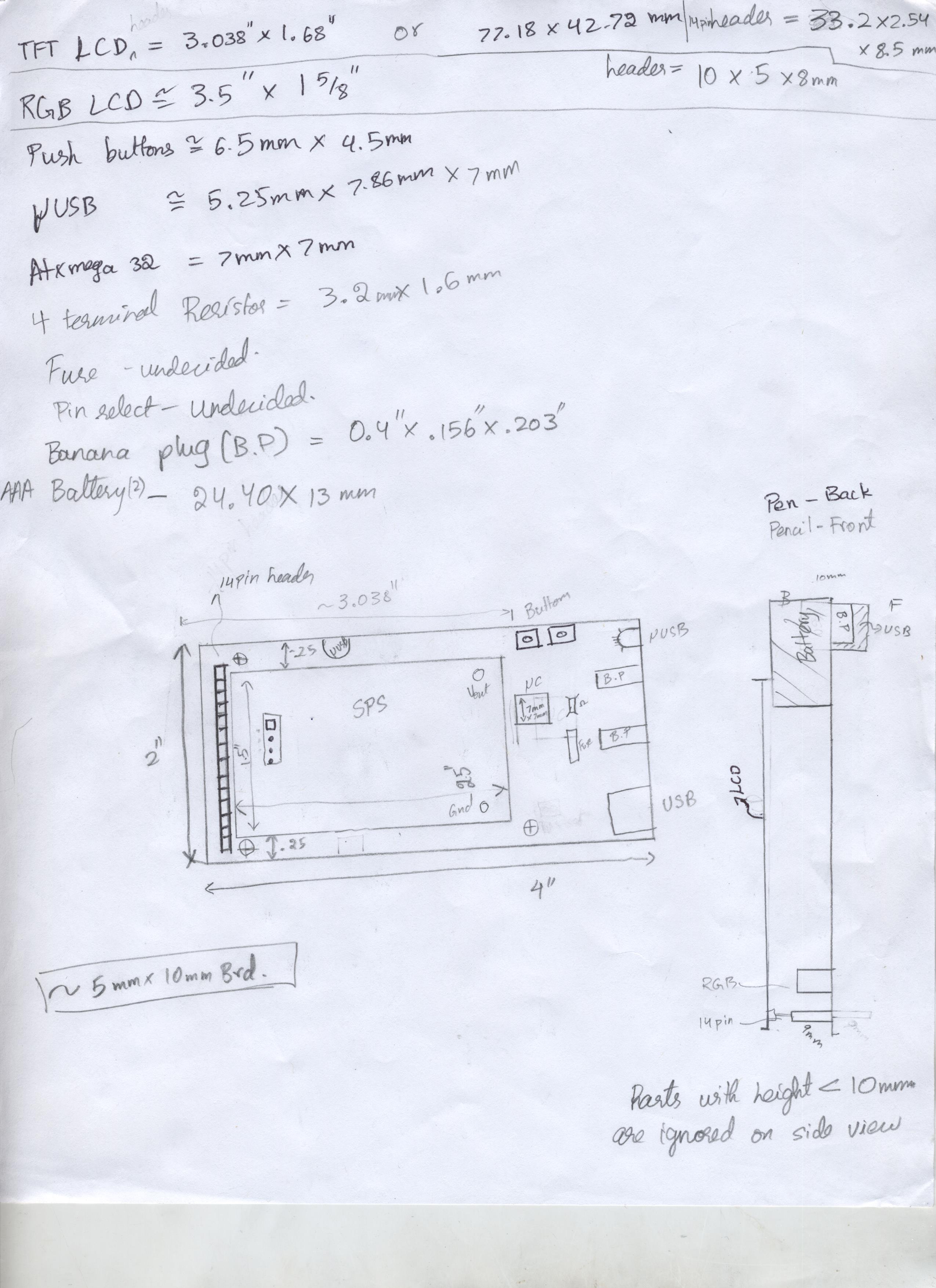
The current meter will be designed to read up to 7A. The maximum current rating is set to be 8A (the fuse will break at this point) and will only be able to read positive DC currents. The circuit can be powered by a battery with a voltage ranging from 2.5 to 5v, in this design 2-AAA battery is used as a power source i.e 3V source. The Analog current measurement will be sampled at 12kSPS (based on atxmega32 specs), and the digital output will have 12-bit resolution.
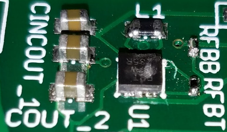
The current is read by measuring the voltage that flows across a shunt resistor. The shunt resistor is specially chosen to have current sense technology, where the resistors packs have 4 terminals, 2 for current flow, and 2 for current measurement. The voltage across the resistor is read using the Atxmega micro controller’s built in Analog to digital converter(ADC).
Since the class is about coming with our own design and specs, I decided to add some extra feature to make this project cooler. A LCD touch screen is added to display the current readings such as peak, instantaneous, rms etc. In addition the LCD will be used to graph continuous data assuming I will finish the programming on time. Since the programming had to go through a number of revisions, a PDI communication will be implemented to modify the code as intended. In addition to serving as a normal current meter, A USB port will be added to monitor the current usage of mobile phone or other devices charged using USB. A micro usb port will be used as the input and USB as output.
Ideal World Scenario
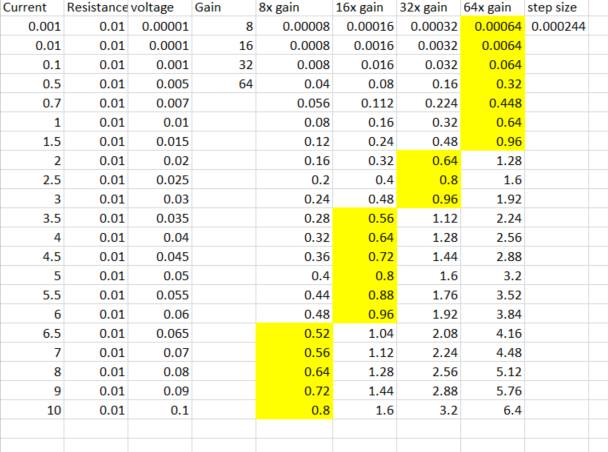
The Atxmega32 comes equipped with amplifier of various ranges like 1/2x, 1x,2x,8x…64x. And since the internal bandgap reference voltage is used, the reference voltage will be a constant 1V. This means by using a 0.01 ohm resistor and using a amplification of 1/2x, the max current that can be read using the meter will be 200A.
Design: Considerations and practical limitations
- Why 7A current limit? The 4 terminal resistors are available for different power rating for 0.01 ohms. For instance, if 5W rated resistor was implemented the maximum current it can handle would be 22.36A (sqrt(5/0.01)). However, larger current required the trace width of the PCB to be more than 0.4 inch/1cm width. Since the board size use for this design is 5cmx5cm, having a trace width of 1cm will require larger board which adds to the cost. In addition the resistor land pattern is quite small that having a trace causes overlaps. A 4mm/.16in trace is implemented in this design, which corresponds to 7-8A according to graph.
 source: https://wiki.xtronics.com/index.php/Wire-Gauge_Ampacity
- Using 0.5mohm vs 1mohm 4 terminal resistor?
Although the cost and sizing of both parts remain the same, for this design 0.01 mohm resistor is used. An ammeter ideally has 0 internal resistance, thus for a current meter design its desired to pick a shunt resistor with lowest resistance. However, I had to go with 1mOhm resistor due to the fact that at practical usage, there is resistance contributed from the solder and traces. This will cause error in measurement. In addition, the limitation also arises from the availability of amplifiers in the MCU. With a step voltage of 0.000244, using 0.5 mOhm resistor will reduce the minimum current that can be measured and also accuracy. Thus to have a smaller minimum current, better accuracy and less error a higher valued resistor was implemented.
- **Implementation of two display ports In addition to a 14 pin header, a 4 pin header is added for i2c communication to provide an alternative display source in case the touch screen display malfunctions and the if the coding cannot be finished on time.
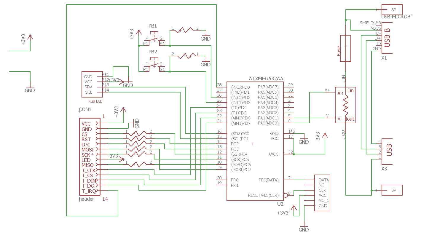
Schematic View
Page one - schematic of the whole circuit with headers, jtag, processor, shunt resistor, fuse, banana plug, usb switches connected and wired according to the requirement.
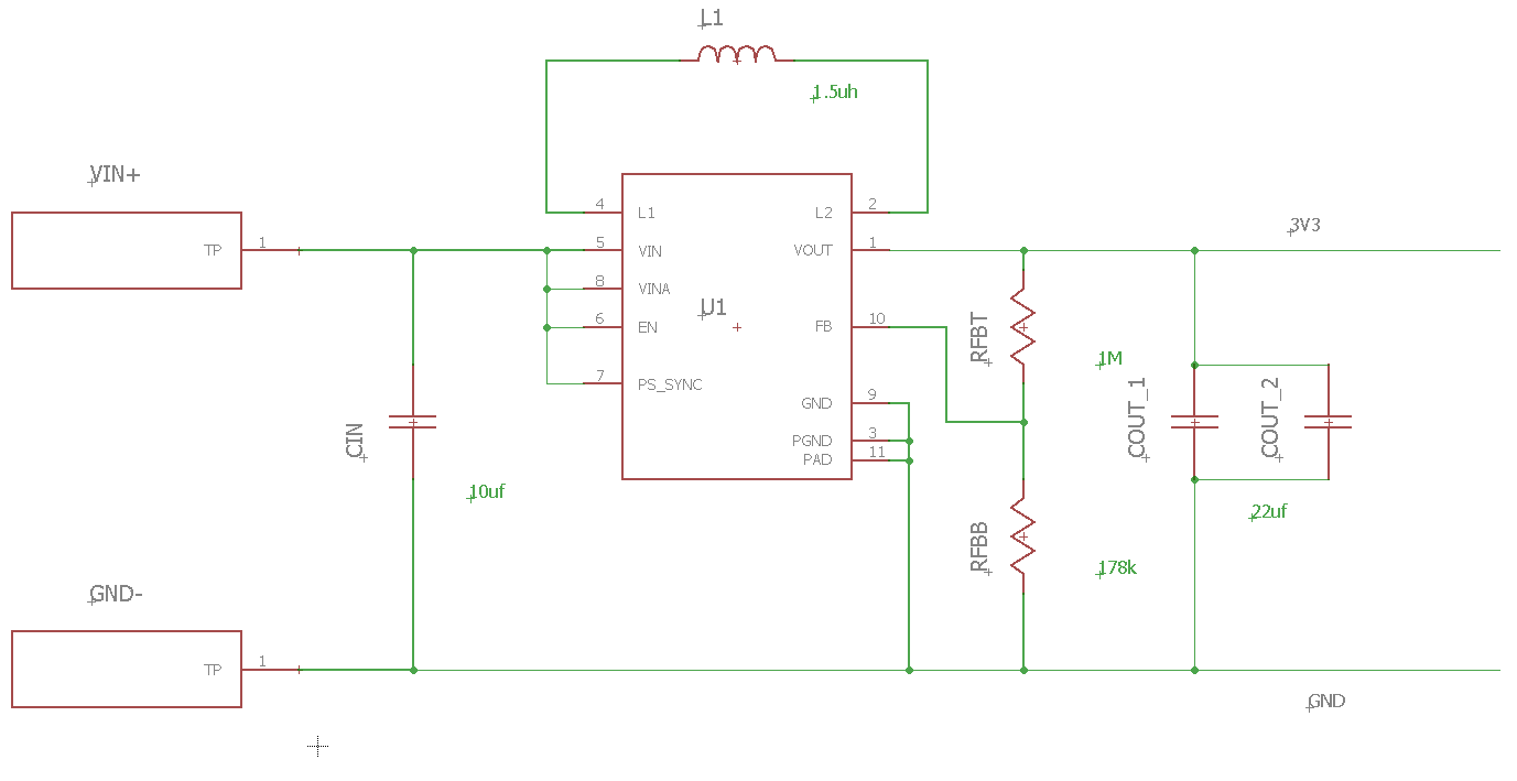
Page two - Schematic drawing of the switching power supply obtained from texas instruments
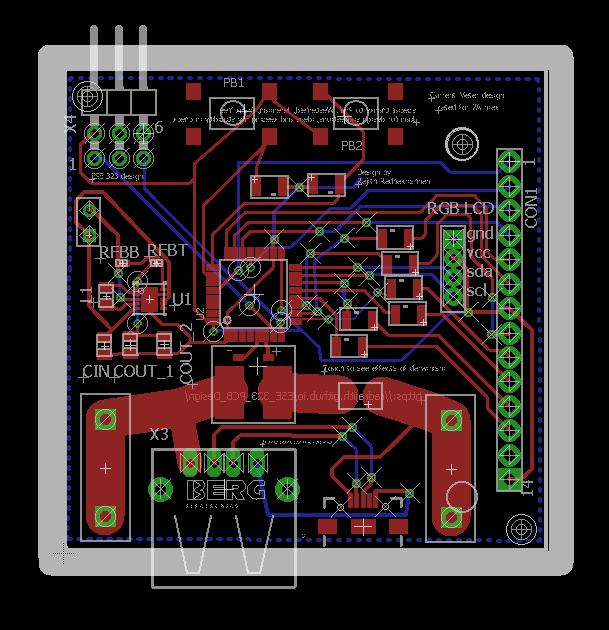
Board view
Board layout
Design rule check and Cam Job
After routing all the parts on the board layout, design rule check had to be used to confirm weather the board meets the requirements. Since Fusion pcb services was planned to be used, the design rule check from seeedstudio was downloaded(DRU link) After running the design rule check, couple of errors was shown. These errors were mainly becuasue of routing wires or vias close to each other. These errors were fixed and the DRC was repeated until there were no errors.
For the cam job, the cam file provided by the seeedstudio does not include one of the files required by the gerbemerge software, it requires a slight modification. The cam file provided from seeedstudio website does not generate “.bor” file required for the gerbmerge software. Download the modified cam file from here. If you choose to modify the cam file provided by seeedstudio by yourself, the instructions are provided after the procedure to create cam files
procedure to create cam files
- In order to do the cam process, on the board window click file > cam processor.
- This will open up a window, Click file > open > job
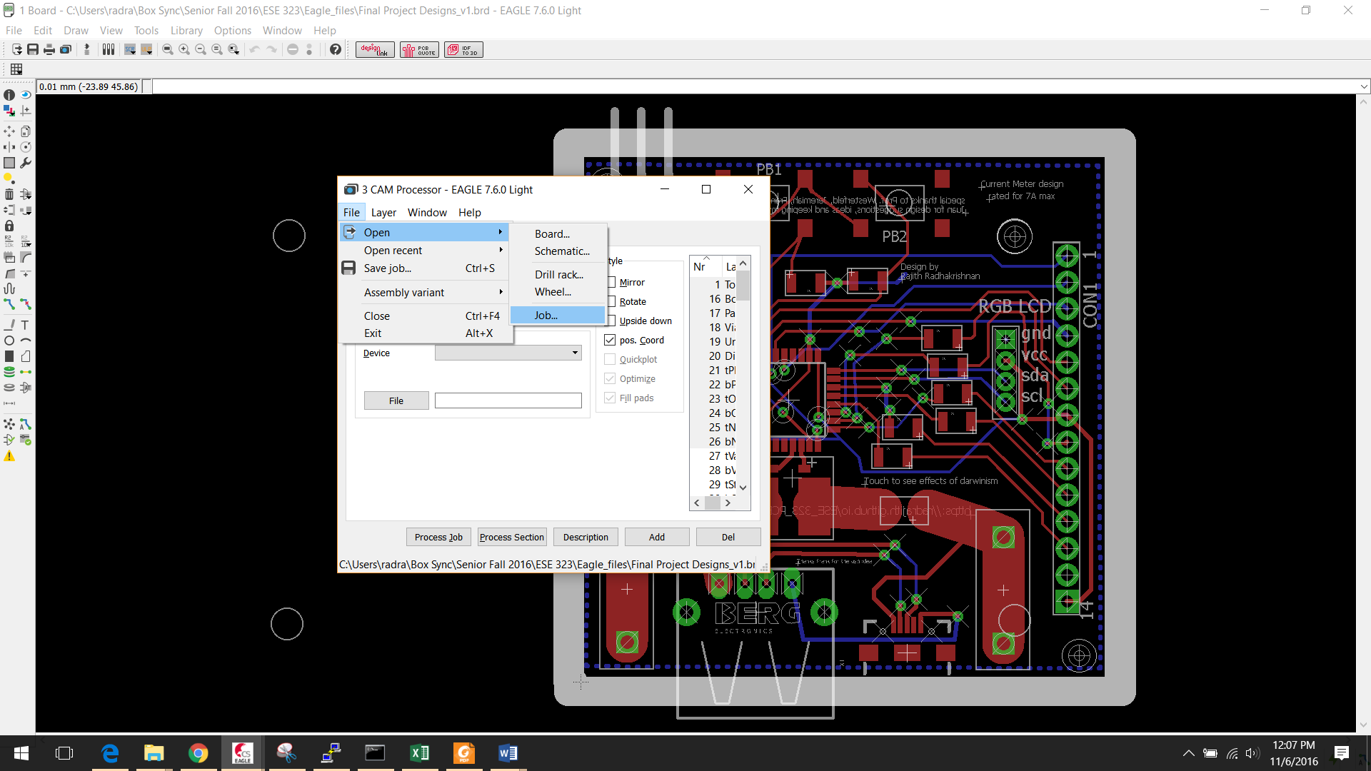
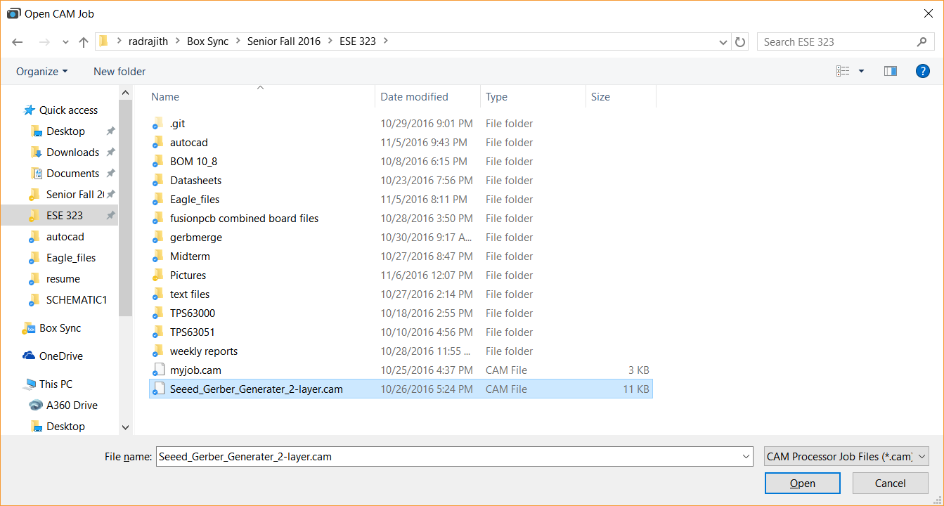
- Locate you cam file downloaded provided in the above paragraph.
- Click process job. This will create all the files necessary to perform gerbmerge operation(described below) or upload to the pcb printing service.
Modify the cam file by yourself(skip this if you used the cam file provided by me)
- After opening the cam processor with the file downloaded from the seeedstudio link, click “add” button
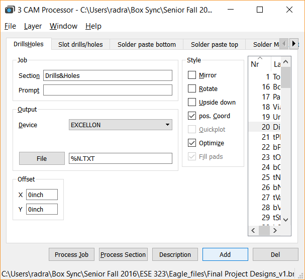
this will create a duplicate window of drill&holes.
- Modify the “Section” from ‘drill&holes’ to ‘board outline’
- Change “device” from ‘excellon’ to ‘GERBER_RS274X’ in the dropdown menu
- Change the “file” extension from ‘.txt’ to ‘.bor’
- On the right side list of layer, make sure only ‘20 dimension’ is selected, scroll all the way to the bottom to make sure.
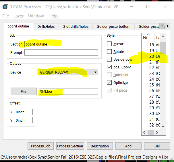
- Click process job. This will create all the files necessary to perform gerbmerge operation(described below) or upload to the pcb printing service.
Printed Circuit Board(merged)
With primary goal of reducing the cost, group of 10 students joined and decided to combine the PCBs and place the order. Seeedstudio’s PCB printint service was used. The 5 Boards were ordered(minimum quantity), for a 260mmX160mm sized board at the cost of $73.65.
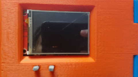
Front view

Rear view
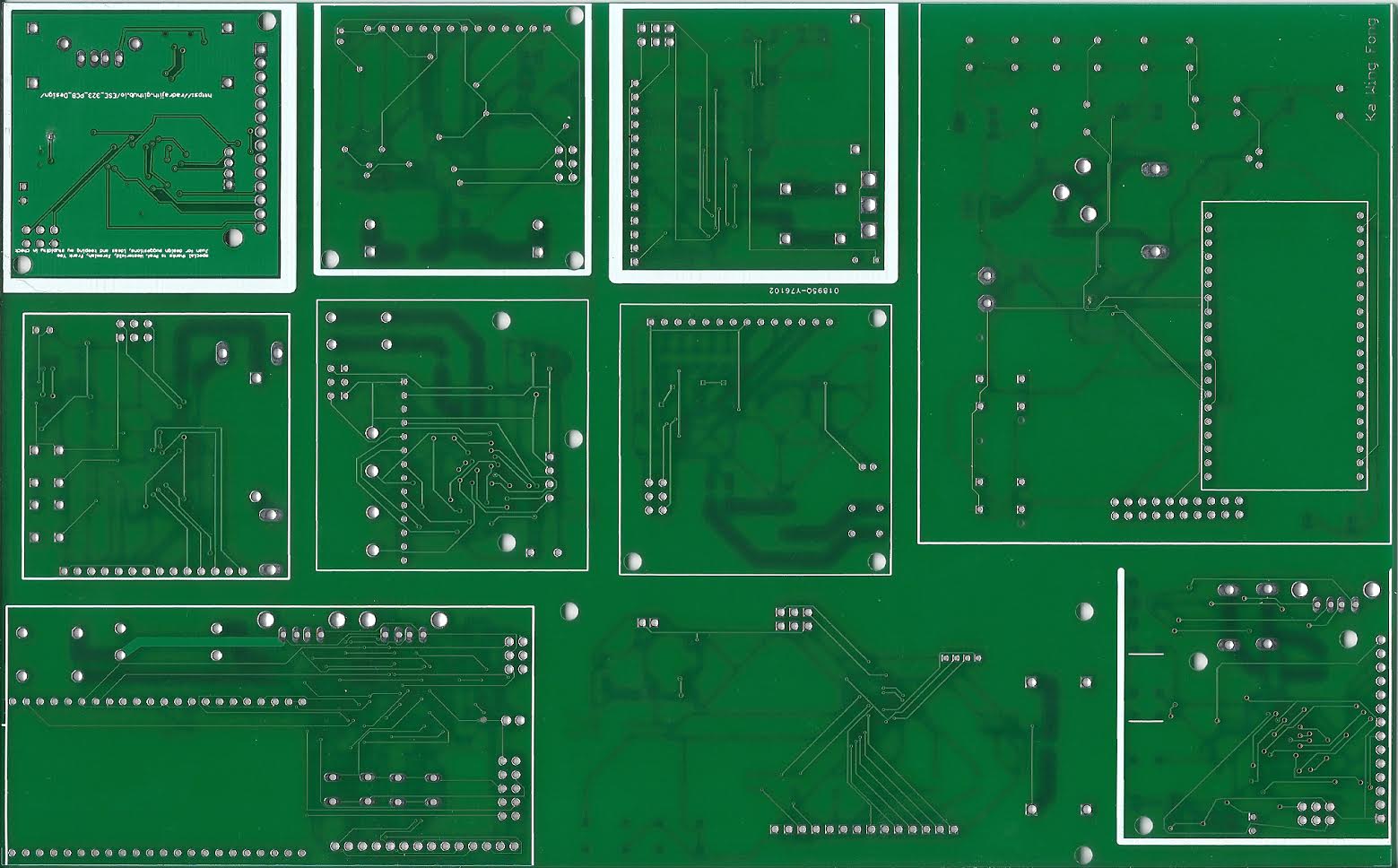
After obtaining the boards, we carefully analyzed for any errors that were made during the manufacturing process. Luckily all of the board were printed as designed in the eagle.
Gerbmerge
For information about gerbemerge and tutorial click here
Thank a lot Frank Yee for helping me make the gerbmerge tutorial and actively contributing to it.
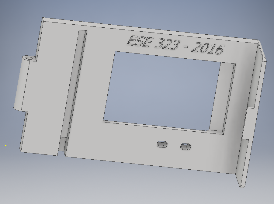
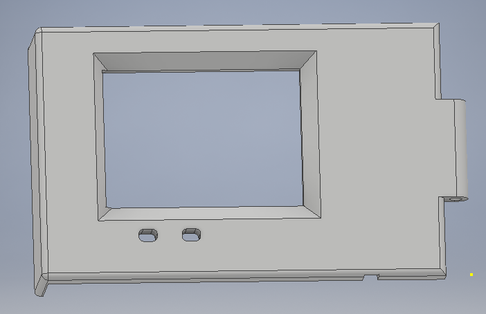
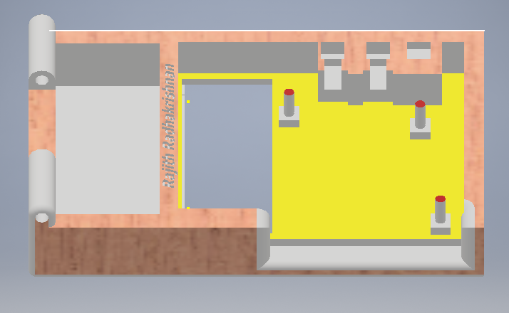
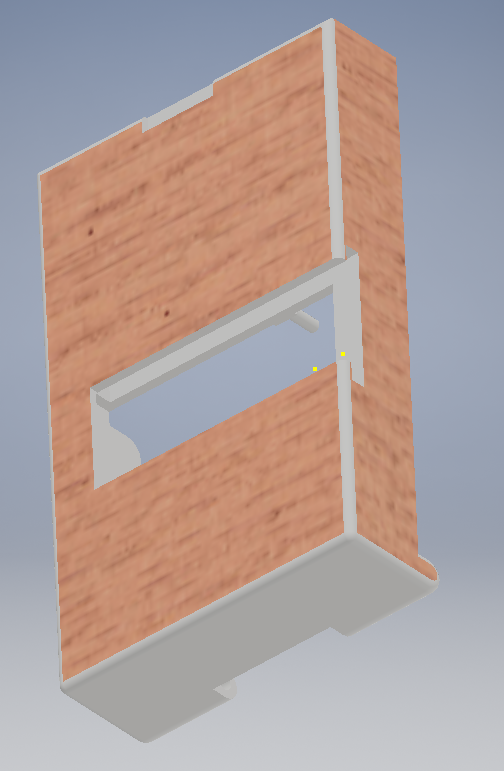
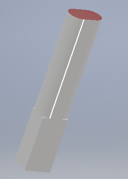
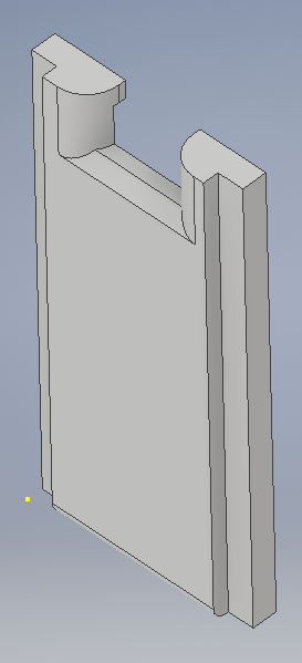
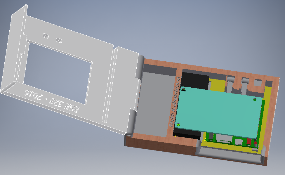
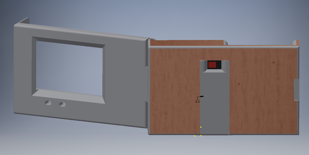
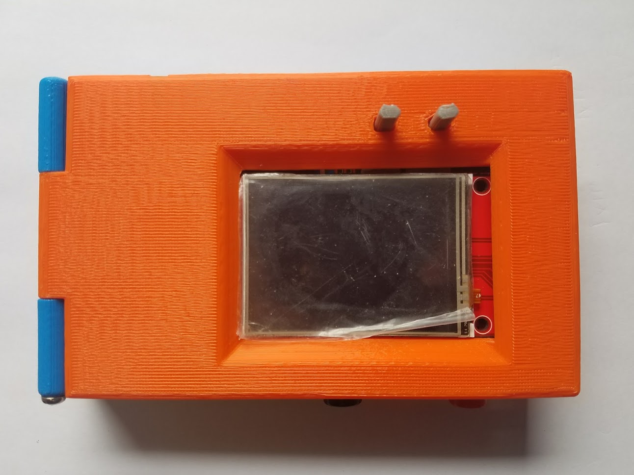
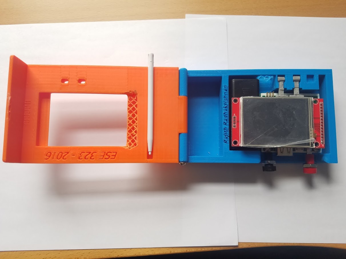
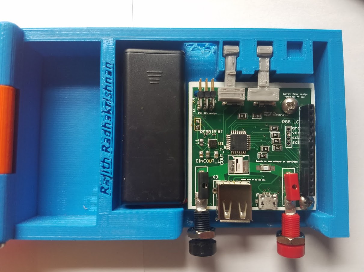
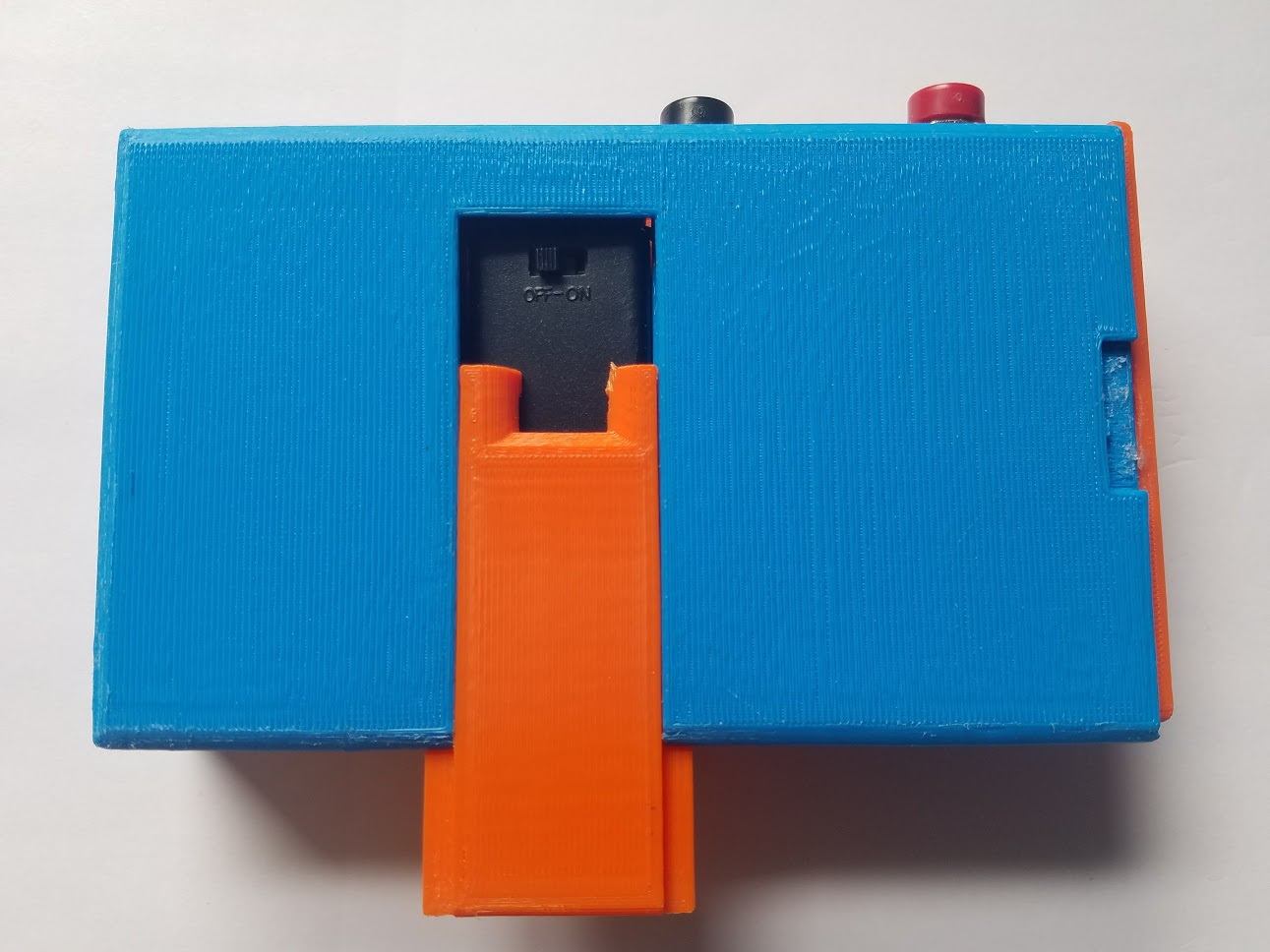
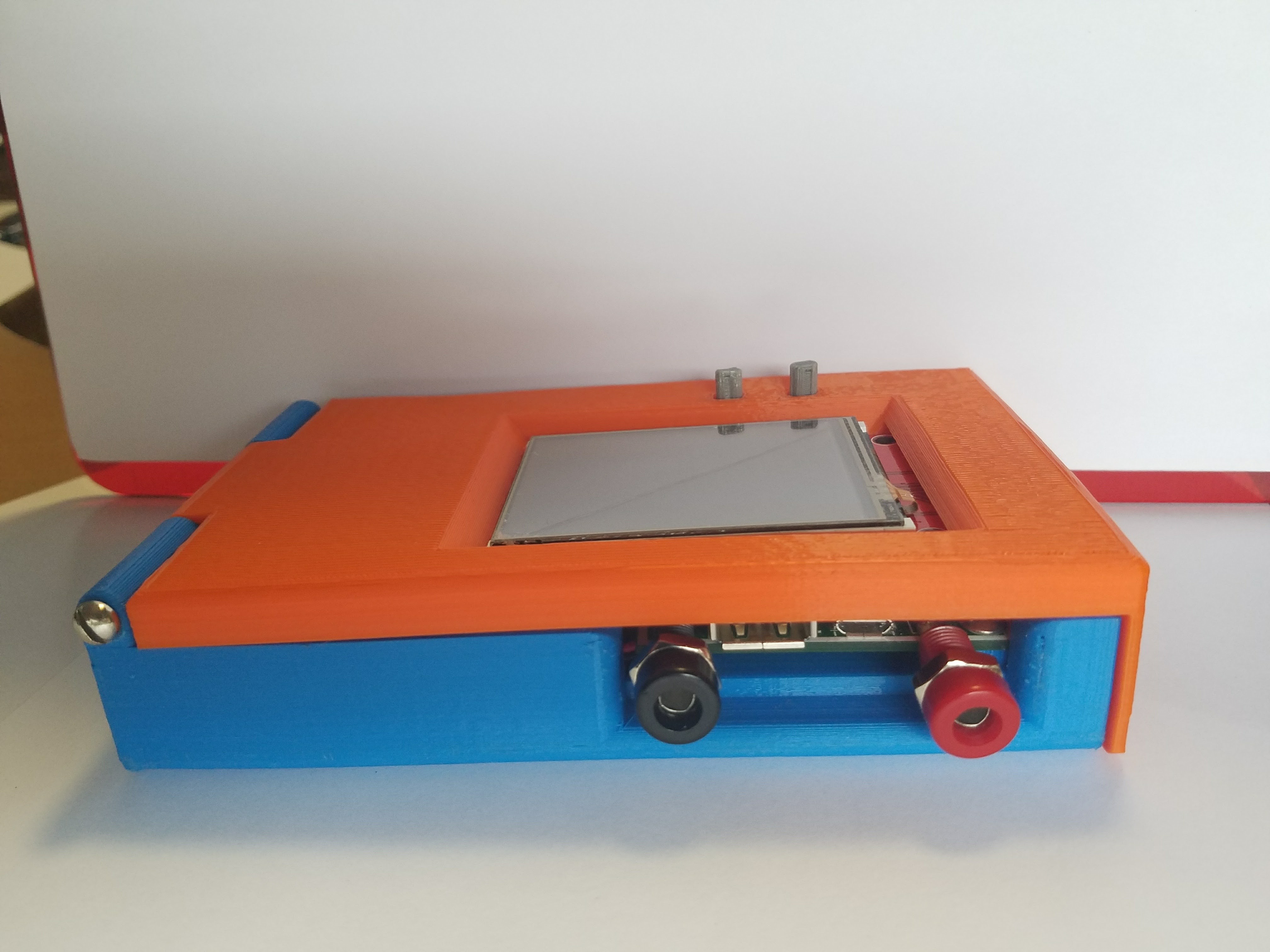
Autodesk Inventor Case design pics
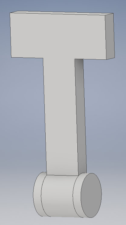
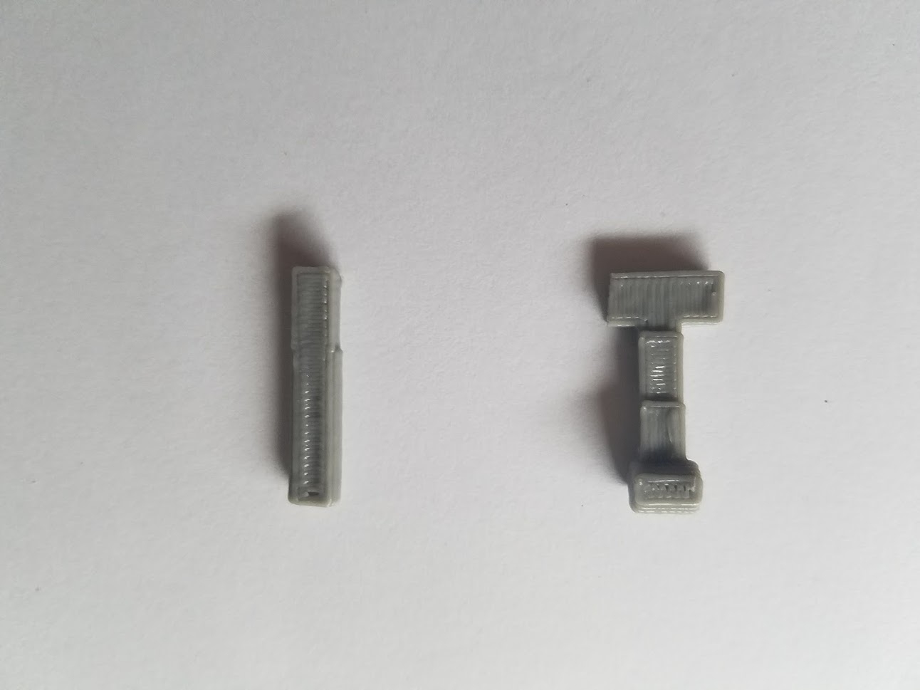
For the case, there were two designs printed. Althougth the first design fit able to encapsulate the board perfectly, there was some inconveniences when changing the battery and assembling the top cover. First design pics The second design was planned to include a slide cover for ease of access to the battery. While programming the LCD screen it was clear that batteries had to be changed often. So accessing battery without disturbing anyother assembly was critical. After designing the first design, it was hard to keep the top case in place, for this reason a door type mechanism was devised and implemented. A stylus slot was added to store when not used, however due to over precision the slot sizing was little small. In addition a hole was added to access Jtag without having to remove the entire board out of the case. Similar to the first design the button press and lever was added to access button present beneath the LCD screen.
- Circuit Board
- Top case
- Bottom case
- Button press extension
- Button press lever
- battery cover
- Assembled parts view.
10 minute video of PCB baking in the oven
To watch the solder melting and skip funny conversation, start at 3.25
finished product
Problems faced and how it was solved
TPS63000 switching power supply assembly
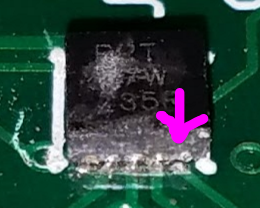
The switching power supply package is 3mmx3mm. Since the schematic and the board layout were obtained from texas instruments(webbench), the true size of the pads and the package were not realized until we saw the pcb. Soldering this package was causing the major problem. Since the solder paste used was coarse, the solder paste did not flow thorough the thinnest needles. Multiple approaches were tried and we finally figured out the best way to solder this package.
As seen in the picture below, although the pins look like they are making contact with pad, in reality they were not connecting. This flaw was figured out thanks to the amazing camera and zoom capabilities of the Samsung galaxy S7(the model without the automatical combustion feature). The microscope present in the lab was not able to provide a clear picture.
-
Approach one laying a bead of solder on the pads and hoping the solder mask will repel and prevent bridging. This approach almost never worked.
-
Approach two
placing a line of solder on a paper towel, making a knife like stucture using paper and placing the exact amount on the pads. This process was highly time consuming and required patience and skills. [Credits - method invented by Harvey and Ricky]
-
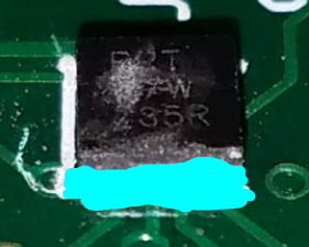
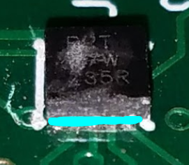
Approach three (success 100%) Instead of relying on the reflow oven to melt the solder paste and make connections, the hot air gun was utilized. Intially the center pad of the SPS was soldered on either using the heatgun or reflow oven(center pad marked in pic 1 below using magenta pen). Once the SPS is correctly placed and firmly secured at the center pad. A bead of solder had to applied on the pins(pic 2). Take a napkin and wipe the SPS all around. Since the package is very small, when the excess is cleaned, a line of solder paste is left handing in the corner(pic 3). Setting the hot air gun to 300 degrees, the hot air was direcly blown on top of the SPS until the solder paste turned shiny(5-10s). Pic 4 shows the clean connection joints made, a amazing zoom skills of Samsung S7.
Pic 1
Pic 2
Pic 3
Pic 4
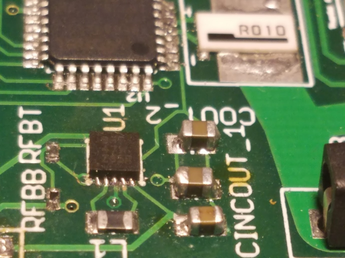
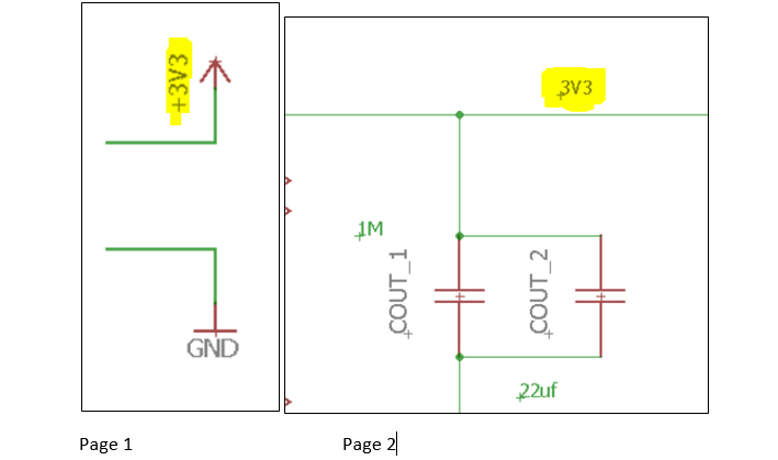
problem in schematic design
when designing the schematic i had two pages. One containing the sps and other containing the rest. When naming the net for vout of the SPS, i named it +3v3 on one page and 3v3 on the other. When reading the net name in page 2, i misread the + that is used to indicate the location, and name the vcc in page 1 as +3v3. This means there was no connecting present in the board.
 This problem was intially fixed by connecting a wire between Cout and the vcc of the jtag.
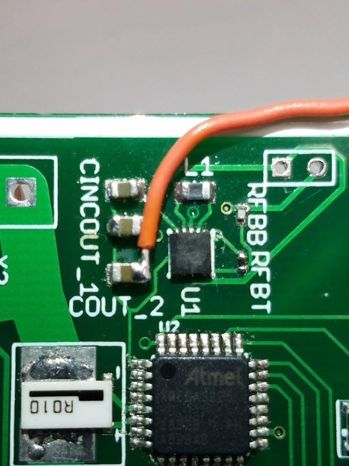
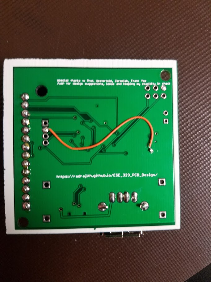
However this fix made the front of my board look ugly. For this reason, i found a via that was coming out on back, and scratched the solder mask off and the metal of the via to make a connection on the back.
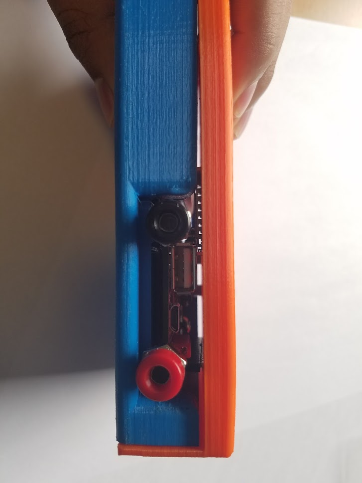
Pushbutton placed underneath the LCD
With the ultimate goal of bringing down the cost, the PCB was designed with the least size (5mmx5mm), thus pushbutton had to be buried underneath the lcd screen. To access the pushbutton the lever type mechanism was implemented in the case design (refer to the button lever picture under the autocad inventor design pics). The foced applied on the button press is transferred to the lever and presses the button.
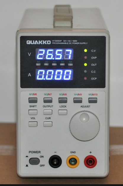
Quakko disaster
While programming the microprocessor, due to the lcd backlight requiring a lot of current, the battery was draining really quickly. To substitute the battery for a constant voltage source, Quakko power supply was used to supply the voltage. The switching power supply when turned on spiked to large voltage causing the SPS to instantly smoke. Due to this disaster, an additional 10 dollars was added to the BOM to obtain the extra SPS.
Gain Calculations
Highlighted areas indicate the ADC readings. The gain will decrease as the voltage reading goes over 0.96V.
Coding
Although major coding is yet to be done, the welcome screen code is currently running on the board. In coming days the touch screen functionality will be implemented along with push button functionality. The ADC code is almost complete, with minor fixes the current meter reading can be done. Ideas for a snake game is partially coded. The coding that has been done so far has been included below Code
Problems faced and coding experience details will be added in the coming days.
Parts, pinouts, BOM
The detailed picture of the parts used has been seperated into a different page along with the BOM. Parts, pinouts, BOM
Since the order of the 10 people were combined, the link to the Super BOM is also attached below. Super BOM
Once again, credits to Frank Yee for putting together and combining the BOM and also managing the finances.
Cost spent
- PCB Board
size - 160mmx260mm
quantity - 5
Cost - $59.92
Shipping - $19.72
Discount - -$5.99
Total - $73.65
- Digikey order
66 parts
Cost - $129.87
Shipping - $13.50
Tax - $12.37
Total - $155.74
- Texas Instruments order
TPS63000
Quantity - 10
Cost - $1.91
Total - $19.10
- Total Money spent
| Rajith | 48 |
| Harvey | 35 |
| Frank | 31 |
| Thomas | 32 |
| Ka Wing | 49 |
| Raymond | 29 |
| Jerry | 27 |
| Daniel | 40 |
| Juan | 22 |
| Ricky | 28 |
| total | 341 |
overall the total cost of the whole project was $48. If some precautionary measure were taken to avoid the quakko disaster, the cost can be reduced $38. If Easyeda pcb printing service was used, the cost could have been reduced further to $34.
Course improvement suggestions
- Finer solder paste to be used with the thinnest needle.
- Encouraging to form groups to bring down the cost of the project
- Deadlines to force student to finish the board designs on time.
- Warn the students about the package sizing, but dont ban the usage of tiny and impossible package. Lets student make mistakes and force them to come up with good solutions.
- Good microscope or Samsung galaxy S7 phone available in the lab to obtain a magnified view of the connection in the PCB
- Processor with larger memory
Contact
radrajith@gmail.com (2016)